Advanced Microscopy Laboratory
Advanced Microscopy Facilities at SPRC
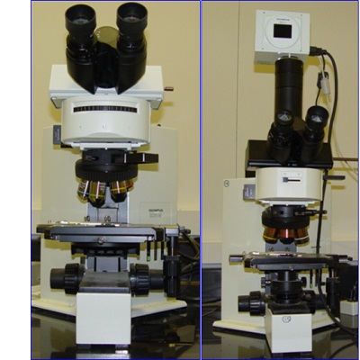
Optical Microscopes, Olympus BX 60M, 500X It gives us an immediate view of plastic parts or resin's visual appearance. It is appropriate for a quick examination. However, it lacks the capability of extended depth-of-field. For applications that need high depth-of-field, SEM is used. Typical usages of OMs are for fracture surface examination, geometrical appearance of resins or parts and for photo-elasticity applications when the accessories are available. |
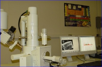
Scanning Electron Microscope (SEM) with EDX, Joel, JSM 6360A A tool to observe an invisible tiny object in a stereographic image with a magnified scale (surface morphology). It has applications in identifying the material structures, surface defects, thickness measurement, stains and residues in materials area. Typical use of EDX is to identify the elements present in the sample. Non-conductive samples are coated with gold by using JEOL JFC-1600 auto fine coater to avoid charge accumulation affecting the image quality. |
|
It is equipped with a 120 kV emitter to achieve a high contrast images for soft matter specimens. TEM microscope provides a detailed image of the inside of a specimen on a nanometer scale. It has applications in a wide range of disciplines, from biology to materials researches, such as biological sections, polymers, nanomaterials, etc. TEM with Energy Dispersive X-ray analysis (EDX) can help in identifying the correct sample features by means of chemical analysis.
|
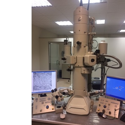 Transmission Electron Microscopy; JEOL JEM-1400